RTP LIVE RESMI
Download Aplikasinya dan Belanja Sekarang!

Success! Please check your phone for the download link
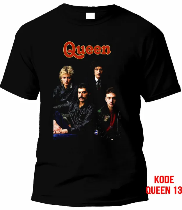
SCATTER HITAM
Sultan4d
LACAK PESANAN

Kategori
- Peralatan Elektronik
- Aksesoris Elektronik
- Fashion & Aksesoris Wanita
- Fashion & Aksesoris Pria
- Fashion & Aksesoris Anak
- Kesehatan & Kecantikan
- Bayi & Mainan
- TV & Elektronik Rumah
- Keperluan Rumah & Gaya Hidup
- Kebutuhan Rumah Tangga
- Olahraga & Outdoor
- Otomotif
- Baju Muslim
- Pakaian Dalam
- Sepatu Pria
- Aksesoris
- Tas Pria
- Perhiasan Pria
- Jam Tangan Pria
- Pakaian Anak Laki-laki
- Pakaian Anak Perempuan
- Pakaian Anak Muslim Laki-Laki
- Pakaian Anak Muslim Perempuan
- Sepatu Anak Laki-laki
- Sepatu Anak Perempuan
- Tas Anak
- Perhiasan Anak
- Jam Tangan Anak
- Perawatan Kulit
- Makeup
- Perawatan Rambut
- Perawatan Tubuh
- Perawatan Diri
- Parfum
- Alat Kecantikan
- Suplemen Makanan
- Alat Medis
- Sexual Wellness
- Perawatan Pria
- Popok Dewasa
- Ibu & Anak
- Popok Sekali Pakai
- Makanan Bayi & Balita
- Pakaian & Aksesoris
- Perlengkapan Menyusui
- Perlengkapan Bayi
- Kamar Bayi
- Perawatan Bayi
- Mainan
- Mainan Elektronik & RC
- Mainan Olahraga & Luar Ruangan
- Mainan Bayi & Balita
- TV & Perangkat Video
- Peralatan Dapur Kecil
- Elektronik Rumah Besar
- Penyejuk dan Pembersih Udara
- Penghisap Debu & Perawatan Lantai
- Alat Perawatan Diri
- Aksesoris & Suku Cadang
- Aksesoris Televisi
- Home Entertainment
- Dekorasi Rumah
- Furnitur
- Kelengkapan Tempat Tidur
- Penerangan
- Peralatan Mandi
- Alat Dapur
- Binatu & Alat Kebersihan
- Perkakas & Perbaikan Rumah
- Kebun & Luar Ruangan
- Alat Tulis & Kerajinan
- Media, Musik & Buku
- Minuman
- Bahan & Bumbu Masakan
- Cokelat, Camilan & Permen
- Makanan Sarapan, Sereal & Selai
- Buah & Sayur
- Kebutuhan Rumah Tangga
- Makanan Hewan Peliharaan
- Aksesoris Hewan Peliharaan
- Kesehatan Hewan Peliharaan
- Baju Olahraga Pria
- Baju Olahraga Wanita
- Sepatu Olahraga Pria
- Sepatu Olahraga Wanita
- Camping dan Hiking
- Peralatan Memancing
- Olahraga Sepeda
- Olahraga Air
- Gym, Yoga & Fitness
- Olahraga Raket
- Perlengkapan Olahraga
- Perlengkapan Sepak Bola
- Suku Cadang & Peralatan Mobil
- Aksesoris Interior Mobil
- Aksesoris Exterior Mobil
- Kamera Mobil, Audio & Video
- Perawatan & Pengkilat Mobil
- Ban & Velg Mobil
- Oli & Cairan Mobil
- Perlengkapan Berkendara & Helm
- Suku Cadang & Peralatan Motor
- Aksesoris & Elektronik Motor
- Ban, Velg, Oli & Cairan Motor
- Kendaraan
Kategori
- Peralatan Elektronik
- Aksesoris Elektronik
- Fashion & Aksesoris Wanita
- Fashion & Aksesoris Pria
- Fashion & Aksesoris Anak
- Kesehatan & Kecantikan
- Bayi & Mainan
- TV & Elektronik Rumah
- Keperluan Rumah & Gaya Hidup
- Kebutuhan Rumah Tangga
- Olahraga & Outdoor
- Otomotif
- Aksesoris Handphone
- Aksesoris Komputer
- Audio
- Aksesoris Berteknologi
- Aksesoris Kamera
- Penyimpanan Data
- Printer
- Aksesoris Tablet
- Komponen Komputer
- Pakaian Wanita
- Baju Muslim
- Lingerie, Baju Tidur & Santai
- Sepatu Wanita
- Aksesoris
- Tas Wanita
- Perhiasan Wanita
- Jam Tangan Wanita
- Pakaian Pria
- Baju Muslim
- Pakaian Dalam
- Sepatu Pria
- Aksesoris
- Tas Pria
- Perhiasan Pria
- Jam Tangan Pria
- Pakaian Anak Laki-laki
- Pakaian Anak Perempuan
- Pakaian Anak Muslim Laki-Laki
- Pakaian Anak Muslim Perempuan
- Sepatu Anak Laki-laki
- Sepatu Anak Perempuan
- Tas Anak
- Perhiasan Anak
- Jam Tangan Anak
- Perawatan Kulit
- Makeup
- Perawatan Rambut
- Perawatan Tubuh
- Perawatan Diri
- Parfum
- Alat Kecantikan
- Suplemen Makanan
- Alat Medis
- Sexual Wellness
- Perawatan Pria
- Popok Dewasa
- Ibu & Anak
- Popok Sekali Pakai
- Makanan Bayi & Balita
- Pakaian & Aksesoris
- Perlengkapan Menyusui
- Perlengkapan Bayi
- Kamar Bayi
- Perawatan Bayi
- Mainan
- Mainan Elektronik & RC
- Mainan Olahraga & Luar Ruangan
- Mainan Bayi & Balita
- TV & Perangkat Video
- Peralatan Dapur Kecil
- Elektronik Rumah Besar
- Penyejuk dan Pembersih Udara
- Penghisap Debu & Perawatan Lantai
- Alat Perawatan Diri
- Aksesoris & Suku Cadang
- Aksesoris Televisi
- Home Entertainment
- Dekorasi Rumah
- Furnitur
- Kelengkapan Tempat Tidur
- Penerangan
- Peralatan Mandi
- Alat Dapur
- Binatu & Alat Kebersihan
- Perkakas & Perbaikan Rumah
- Kebun & Luar Ruangan
- Alat Tulis & Kerajinan
- Media, Musik & Buku
- Minuman
- Bahan & Bumbu Masakan
- Cokelat, Camilan & Permen
- Makanan Sarapan, Sereal & Selai
- Buah & Sayur
- Kebutuhan Rumah Tangga
- Makanan Hewan Peliharaan
- Aksesoris Hewan Peliharaan
- Kesehatan Hewan Peliharaan
- Baju Olahraga Pria
- Baju Olahraga Wanita
- Sepatu Olahraga Pria
- Sepatu Olahraga Wanita
- Camping dan Hiking
- Peralatan Memancing
- Olahraga Sepeda
- Olahraga Air
- Gym, Yoga & Fitness
- Olahraga Raket
- Perlengkapan Olahraga
- Perlengkapan Sepak Bola
- Suku Cadang & Peralatan Mobil
- Aksesoris Interior Mobil
- Aksesoris Exterior Mobil
- Kamera Mobil, Audio & Video
- Perawatan & Pengkilat Mobil
- Ban & Velg Mobil
- Oli & Cairan Mobil
- Perlengkapan Berkendara & Helm
- Suku Cadang & Peralatan Motor
- Aksesoris & Elektronik Motor
- Ban, Velg, Oli & Cairan Motor
- Kendaraan